
In the southern Dutch city of Veldhoven, near the Belgian border, is the only factory capable of assembling a revolutionary machine that the world’s largest chipmakers rely on.
EUV lithography is the most expensive step in the manufacture of advanced microchips that power data centres, cars and iPhones. The machines are made by a single company: Advanced Semiconductor Materials Lithography.
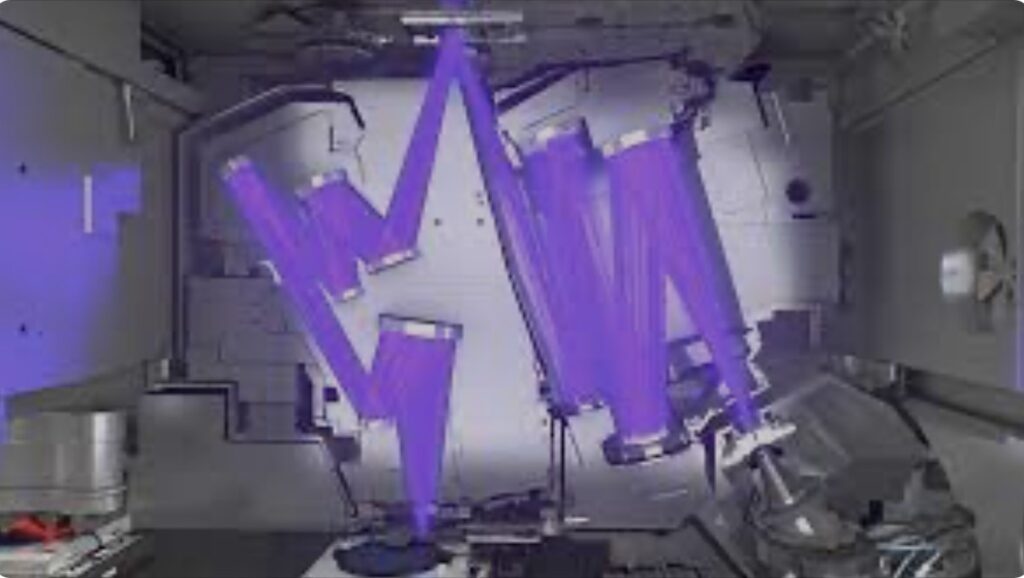
“ASML has a monopoly on manufacturing EUV lithography machines, the most advanced type of lithography equipment needed to make every advanced processor chip we use today,” said Chris Miller, assistant professor at the Fletcher School at Tufts University. “The machines they produce, each of them are among the most complicated devices ever made.”
EUV stands for extreme ultraviolet, an incredibly short wavelength of light that ASML generates in large quantities to print small, complex designs on microchips. EUV light is created by tiny bursts of molten tin that occur at extreme speeds and then bounce off Zeiss’ unique mirrors, which ASML claims are the flattest surface in the world. A small percentage of the EUV light particles reach the surface of a silicon wafer, where they imprint the tiny designs that determine what each chip will do.
Extreme ultraviolet (EUV) lithography is a chip manufacturing technology that uses extreme ultraviolet light to etch extremely fine patterns on silicon wafers. This technology is key to the production of semiconductors with process nodes of 3nm (nanometres) or even smaller. Some of the highlights of how EUV facilitates this are described below:
Shortest Wavelength
EUV uses a much shorter wavelength (around 13.5nm) compared to deep ultraviolet (DUV) lithography, which typically uses wavelengths in the 193nm range. A shorter wavelength allows for higher precision and resolution, which is essential for scaling up to smaller process nodes such as 3nm.
Fewer Multi-Pattern Steps
In older methods, complex designs often required multiple exposure steps to create a single layer of a chip. EUV significantly reduces the need for these “multi-patterning” steps, which not only speeds up the manufacturing process but also improves accuracy.
Improvements to the Resist Layer
The resist is the light-sensitive layer that is applied to the wafer and exposed to create patterns. Resist formulations for EUV have improved in terms of sensitivity and resolution, which is critical to enable smaller node sizes.
Improved Light Source Systems
Light source systems for EUV are extremely complex and require precise control to maintain a coherent and stable light output. Improvements in these systems have made mass production using EUV feasible.
Controlling defects
The shorter wavelength and more precise process also mean that EUV is more sensitive to defects. However, advances in defect inspection and repair have kept pace, allowing very high quality control even at scales of 3nm or less.
Economic and Performance Advantages
Chips fabricated with 3nm process nodes offer significantly improved performance and power efficiency compared to their larger counterparts. This translates into faster and more energy-efficient devices, from servers to mobile devices.
In short, EUV is a crucial technology that has enabled the extreme miniaturisation of transistors on silicon chips, facilitating the manufacture of 3nm and smaller semiconductors.
ASML CEO Peter Wennink said the company has been driving down semiconductor prices since it was founded 38 years ago and will continue to do so “for the next two decades”.
“The world needs more chips,” Wennink told CNBC. “So we need to make more machines which, by the way, will continue to increase in average selling price as long as we can reduce the cost per transistor.”
ASML has sold a total of about 140 EUV systems in the past decade, each of which now costs up to $200 million, according to Wennink. The price tag for its next machine, called High NA, will be more than $300 million.
Its EUV machine is “so expensive that most companies can’t afford it,” says Joanne Itow, managing director of manufacturing at Semico Research. “It has certainly knocked a lot of suppliers out of the market,” including chipmaker GlobalFoundries, which decided a few years ago to stop working on more advanced chips because of the high cost, she said.